
Table of Contents
8085 Microprocessor
8085 Microprocessor, commonly known as “Eighty Eighty-Five Microprocessor” is an 8-bit microprocessor introduced by Intel in 1977. It is part of the 8080 Microprocessor family and is one of the most popular and widely used microprocessors in the early days of microcomputing. The 8085 Microprocessor played a crucial role in the development of early personal computers and embedded systems.
The 8085 Microprocessor is based on an 8-bit architecture i.e. it can process data and instructions in 8-bit chunks. It has a 16-bit address bus, which allows it to address up to 64KB of memory. All the information related to the 8085 Microprocessor like its architecture, pin diagram, interrupt, etc. is covered in this article in a precise and understandable manner.
8085 Microprocessor Architecture
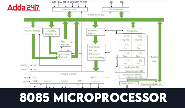
The 8085 Microprocessor Architecture encompasses various function units that play a crucial role in the design and functionality of the 8085 Microprocessor. The 8085 Microprocessor Architecture is explained below for the student’s ease.
Accumulator (A)
The accumulator is an 8-bit register used for performing various arithmetic and logical operations. It is the primary register for most calculations in the processor i.e. the data is by default stored in it only.
Program Counter (PC)
The 16-bit program counter keeps track of the memory address of the next instruction to be executed. It is automatically incremented after each instruction fetch.
Stack Pointer (SP)
The 16-bit stack pointer keeps track of the memory location where data is stored during subroutine calls and stack operations. It is used in conjunction with the stack to manage program execution and return addresses.
General-Purpose Registers
The 8085 microprocessor consists of six general-purpose 8-bit registers (B, C, D, E, H, L) that can be used for data manipulation and storage. These registers can also be used in pairs (BC, DE, HL) to handle 16-bit data.
Flag Register
The flag register contains various condition flags that indicate the result of arithmetic and logical operations. These flags include the Zero Flag (Z), Sign Flag (S), Parity Flag (P), Carry Flag (CY), and Auxiliary Carry Flag (AC). These flags are crucial for branching and conditional execution of instructions.

Arithmetic and Logic Unit (ALU)
The ALU is responsible for performing arithmetic and logical operations on data stored in registers, including addition, subtraction, AND, OR, XOR, and more.
Control Unit
The control unit coordinates the execution of instructions by generating control signals for various components, such as the ALU, registers, and memory. It fetches instructions from memory, decodes them, and executes them in the appropriate sequence.
Instruction Register and Decoder
It is an 8-bit register used to fetch instructions from memory then it is stored in the Instruction register. The instruction decoder decodes the information present in the Instruction register.
Memory Interface
The 8085 microprocessor has a 16-bit address bus (AD0-AD15) and an 8-bit data bus (D0-D7) for communication with external memory devices. It can address up to 64KB of memory.
Input/Output (I/O) Ports
The 8085 microprocessor includes instructions and hardware for input and output operations. It can communicate with peripheral devices through I/O ports.
Interrupt Control
The 8085 microprocessor supports various interrupt signals (INTR, RST 7.5, RST 6.5, RST 5.5, and TRAP) that allow external devices to interrupt normal program execution.
Clock Generator
The 8085 microprocessor requires an external clock signal to synchronize its operations. The clock speed typically ranges from 2.0 to 3.2 MHz in different variants.
Power Supply
The 8085 microprocessor typically operates on a +5V DC power supply.
The execution of instructions in the 8085 microprocessor involves fetching an instruction from memory, decoding it, executing the specified operation, and updating the relevant registers and flags as needed. The architecture of the 8085 is designed to support a wide range of data processing and control tasks and was widely used in early microcomputer systems and embedded applications.

8085 Microprocessor Pin Diagram
8085 Microprocessor is a 40-pin microprocessor that defines how it connects to other components and devices. Here is a simplified pin diagram for the 8085 microprocessor. Here is a brief description of some of the important pins:
- VCC (+5V): Power supply pins, the 8085 microprocessor typically operates on a +5V DC power supply.
- CLKOUT: Clock output pin, used to provide the clock signal for other devices.

- INTR: Interrupt Request, External devices can use this pin to request an interrupt.
- HOLD and HLDA: Hold and Hold Acknowledge pins. Used for DMA (Direct Memory Access) operations.
- INTA: Interrupt Acknowledge. It indicates that the microprocessor has acknowledged an interrupt request.
- RESET OUT and RESET IN: Used for resetting the microprocessor.
- X1 and X2: Crystal oscillator input and output pins for connecting an external clock source.
- AD0-AD7: Address/Data Bus. These pins carry both address and data information.
- SID and SOD: Serial Input Data and Serial Output Data pins for serial communication.
- ALE: Address Latch Enable. It is used to latch the address from the address bus during the first clock cycle of a machine cycle.
- TRAP, RST7.5, RST6.5, RST5.5: Pins for handling software and hardware interrupts.
- GND: Ground reference.


 ISRO Scientist/ Engineer Recruitment 202...
 ISRO SAC Admit Card 2026 Out, Direct Dow...
 NBCC JE Answer Key 2026 Out, Download Re...