SSC JE Basic Electronics Questions with Detailed Solutions

Get SSC JE Basic Electronics Questions to prepare for your upcoming exam. Solve the most expected questions and detailed solutions that can be asked in the exam.

Important SSC JE Basic Electronics Questions

Q1.

The Variation in the effective width of a base in a Bipolar Junction Transistor is due to a variation in the applied __________.

  • A.emitter current
  • B.collector current
  • C.emitter to collector voltage
  • D.base to collector voltage
    ✓ Correct
  • E.

    None of these

Answer & Solution

Correct option is D

Concept: The phenomenon called "Early effect" describes how the effective width of a BJT's base changes when the reverse bias voltage across the collector-base junction changes.
Impact of voltage change: When the base-collector voltage increases, the depletion region at the collector-base junction expands, effectively narrowing the base region. This change in base width alters the transistor's current gain. 
Q2.

What are the two types of breakdowns that can occur in p-n junctions?

  • A.

    Voltage and current breakdowns

  • B.

    Forward and reverse breakdowns

  • C.

    Avalanche and tunnelling breakdowns

    ✓ Correct
  • D.

    Zener and capacitive breakdowns

Answer & Solution

Correct option is C

In p-n junctions, breakdowns can occur through two main mechanisms:
1. Avalanche Breakdown: This occurs due to the collision of charge carriers gaining enough energy to cause additional carriers to be released in an avalanche-like process.
2. Tunnelling Breakdown: This occurs when charge carriers quantum tunnel through the depletion region barrier.
So, the correct option is (c) Avalanche and tunnelling breakdowns.

Q3.

Which of the following statements is correct regarding the doping levels of the emitter, base and collector regions in a bipolar junction transistor (BJT)?

  • A.

    The emitter is lightly doped, the base is heavily doped and the collector is moderately doped.

  • B.

    The emitter is heavily doped, the base is lightly doped and the collector is moderately doped.

    ✓ Correct
  • C.

    The emitter is moderately doped, the base is heavily doped and the collector is lightly doped.

  • D.

    The doping levels of the emitter, base and collector are all the same.

Answer & Solution

Correct option is B

- In a bipolar junction transistor (BJT), the emitter is heavily doped to increase emitter current.
- The base is lightly doped to allow for high base resistance.
- The collector is moderately doped to withstand high reverse bias voltage.
- This doping profile helps achieve the desired transistor characteristics.

Q4.

What is the result of the diffusion of electrons and holes when p-type and n-type semiconductor materials are joined to form a diode junction?

  • A.

    Depletion of majority charge carriers in the region near the junction

    ✓ Correct
  • B.

    Generation of an electric field that inhibits electron movement

  • C.

    Creation of a layer of holes near the junction in the p-type material

  • D.

    Formation of positive ions in the p-type material and negative ions in the n-type material

Answer & Solution

Correct option is A

- When p-type and n-type semiconductor materials are joined to form a diode junction, diffusion of majority charge carriers (holes in the p-type and electrons in the n-type) occurs.
- This diffusion leads to the depletion of majority charge carriers in the region near the junction, creating a depletion region.
- The depletion region has a lack of free charge carriers, resulting in the formation of a potential barrier or built-in electric field at the junction.

Q5.

If the value of the common base current gain (α) is 0.98, then the value of the common collector current gain (γ) is ___________.

  • A.

    98

  • B.

    49

  • C.

    0.02

  • D.

    50

    ✓ Correct

Answer & Solution

Correct option is D

Common base current gain, α=0.98

The relationship between common base current gain (α) and common collector current gain (γ) is:

γ=11−αγ=11−0.98=10.02=50Additional Information:Common emitter current gain (β):β=ICIBCommon base current gain (α):α=ICIECommon collector current gain (γ):γ=IEIBWhere,IC=Collector currentIB=Base currentIE=Emitter current\gamma = \frac{1}{1 - \alpha} \\[6pt]\gamma = \frac{1}{1 - 0.98} = \frac{1}{0.02} = 50 \\[10pt]\textbf{Additional Information:} \\[6pt]\text{Common emitter current gain } (\beta): \quad \beta = \frac{I_C}{I_B} \\[6pt]\text{Common base current gain } (\alpha): \quad \alpha = \frac{I_C}{I_E} \\[6pt]\text{Common collector current gain } (\gamma): \quad \gamma = \frac{I_E}{I_B} \\[10pt]\textbf{Where,} \\[4pt]I_C = \text{Collector current} \\[4pt]I_B = \text{Base current} \\[4pt]I_E = \text{Emitter current}​​

Q6.

The voltage gain in common collector configuration of a BJT is _____.

  • A.

    less than one

    ✓ Correct
  • B.

    zero

  • C.

    between 50 and 100

  • D.

    above 100

Answer & Solution

Correct option is A

In a common collector configuration, the output voltage is taken from the collector, and the input is applied to the emitter. The voltage gain in a common collector configuration is slightly less than one. While the voltage gain is modest, this configuration is known for other favorable characteristics like high input impedance and low output impedance.

Q7.

The AC ripples can be reduced in a rectifier circuit by using capacitive filter by _________ the capacitance value and by ________ the input frequency.

  • A.

    increasing; decreasing

  • B.

    increasing; increasing

    ✓ Correct
  • C.

    decreasing; increasing

  • D.

    decreasing; decreasing

Answer & Solution

Correct option is B

• The ripple factor (γ) for a full-wave rectifier using a capacitor filter is given by:

​γ=143RLCf\gamma = \frac{1}{4\sqrt{3}R_LCf}​​

Where:

  • C = capacitance
  • f = input frequency
  • RLR_L​​ = load resistance

To reduce the AC ripples, the capacitance should be increased and the input frequency should also be increased.

This is because the ripple factor (γ) is inversely proportional to both the capacitance and the frequency.

As the capacitance C increases and the frequency f increases, the ripple factor decreases, thus reducing the AC ripples.

Q8.

At higher forward voltages, a junction diode is likely to ________.

  • A.

    become noisy

  • B.

    get saturated

  • C.

    break down

  • D.

    burn out

    ✓ Correct

Answer & Solution

Correct option is D

When a diode is forward biased, increasing the voltage reduces the resistance of the depletion region, allowing more current to flow. However, there's a limit to how much current a diode can handle.
 If the forward voltage exceeds the diode's rated maximum forward voltage, excessive current can flow through the diode, causing it to overheat and potentially damage the junction, leading to a "burn out" condition.

Q9.

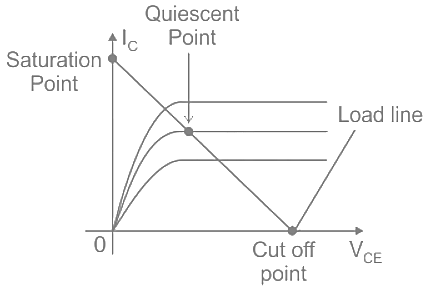
The operating point of a transistor known as _______.

  • A.

    cut-off point

  • B.

    active point

  • C.

    quiescent point

    ✓ Correct
  • D.

    threshold point

Answer & Solution

Correct option is C

 The operating point is also known as the quiescent point in transistor operation, typically defined as the point where the transistor is biased in the absence of any input signal.
 The correct term for the operating point of a transistor is the quiescent point, also referred to as the Q-point. It represents the DC operating point where the transistor is in its steady-state condition before any AC signal is applied.

Q10.

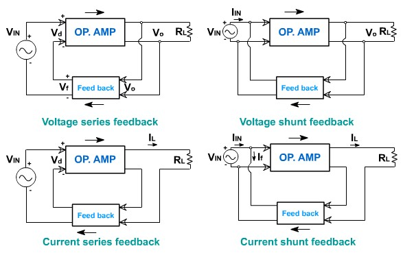
The collector to the base bias configuration of a common emitter transistor implicitly employs:

  • A.

    voltage series positive feedback

  • B.

    voltage shunt negative feedback

    ✓ Correct
  • C.

    current series negative feedback

  • D.

    current shunt negative feedback

Answer & Solution

Correct option is B

Voltage shunt: In this configuration, a portion of the output voltage (collector voltage) is fed back to the input (base) through a resistor, creating a feedback loop. 
Negative feedback: This feedback is negative because it opposes the input signal, stabilizing the circuit and reducing distortion. 
Shunt: The feedback is considered "shunt" because the feedback voltage is applied in parallel with the base resistor. 

Q11.

The built-in potential of a p-n junction __________.

  • A.

    depends on doping concentration only

  • B.

    depends on both temperature and doping concentration

    ✓ Correct
  • C.

    depends on temperature only

  • D.

    does not depend on temperature and doping concentration

Answer & Solution

Correct option is B

From the energy band diagram and the expressions derived, the built-in potential can be calculated as:

​Vbi=VTln⁡(NANDni2)V_{bi} = V_T \ln \left( \frac{N_A N_D}{n_i^2} \right)​​

The built-in potential is affected by both temperature and doping concentration. As temperature increases, the intrinsic carrier concentration nin_i​ increases, which leads to a change in the built-in potential. Similarly, changes in doping concentration NA or NDN_A \text{ or } N_D​ also influence the potential.

where:

​VT=kTqV_T = \frac{kT}{q}​​

(Thermal voltage)

  • NAN_A​  and NDN_D​​ are the doping concentrations for the p and n regions, respectively.
  • nin_i​ is the intrinsic carrier concentration.


​

Q12.

In a semiconductor diode, the ratio of change in the forward biased voltage across the diode to change in the current in the diode is called ________.

  • A.

    DC forward resistance

  • B.

    AC reverse resistance

  • C.

    AC forward resistance

    ✓ Correct
  • D.

    DC reverse resistance

Answer & Solution

Correct option is C

AC forward resistance: This refers to the resistance a diode offers to a small change in current when it is forward biased. This is the ratio of the change in forward voltage to the corresponding change in current. 
DC forward resistance: This refers to the ratio of the DC voltage applied to a diode to the resulting DC current. While related, it is not the same as AC forward resistance. 
AC reverse resistance: When a diode is reverse biased, its resistance is very high. This is because the diode is essentially blocked from conducting current in the reverse direction. Therefore, there is no meaningful "AC reverse resistance" in the same way as with forward bias. 
DC reverse resistance: Similar to AC reverse resistance, this is not a commonly used term as the diode's high resistance under reverse bias makes it essentially infinite for practical purposes. 

Q13.

The current amplification factor for a transistor in a common base configuration is 0.75. If the emitter current is 4A, find the base current.

  • A.

    5 A

  • B.

    1 A

    ✓ Correct
  • C.

    3 A

  • D.

    0 A

Answer & Solution

Correct option is B

Current Gain Relations in Transistors:1. Common emitter current gain (β):β=ICIB2. Common base current gain (α):α=ICIE3. Common collector current gain (γ):γ=IEIBWhere:∙ IE=Emitter current∙ IC=Collector current∙ IB=Base currentCalculation:Given:∙ IE=4 A∙ α=0.75IC=α×IE=0.75×4=3 ANow, using the relation:IE=IC+IB => 4=3+IB => IB=1 A\textbf{Current Gain Relations in Transistors:} \\[8pt]1. \; \text{Common emitter current gain } (\beta): \\\beta = \dfrac{I_C}{I_B} \\[12pt]2. \; \text{Common base current gain } (\alpha): \\\alpha = \dfrac{I_C}{I_E} \\[12pt]3. \; \text{Common collector current gain } (\gamma): \\\gamma = \dfrac{I_E}{I_B} \\[14pt]\text{Where:} \\\bullet \; I_E = \text{Emitter current} \\\bullet \; I_C = \text{Collector current} \\\bullet \; I_B = \text{Base current} \\[12pt]\textbf{Calculation:} \\[6pt]\text{Given:} \\\bullet \; I_E = 4 \, A \\\bullet \; \alpha = 0.75 \\[10pt]I_C = \alpha \times I_E = 0.75 \times 4 = 3 \, A \\[12pt]\text{Now, using the relation:} \\I_E = I_C + I_B \;\;\Rightarrow\;\; 4 = 3 + I_B \;\;\Rightarrow\;\; I_B = 1 \, A​​

Q14.

In a metal oxide semiconductor FET, the metal oxide layer acts as a/an _________.

  • A.

    electric field

  • B.

    capacitor

  • C.

    dielectric

    ✓ Correct
  • D.

    gate

Answer & Solution

Correct option is C

In a metal oxide semiconductor field-effect transistor (MOSFET), the metal oxide layer, typically made of silicon dioxide (SiO₂), acts as a dielectric material. It separates the gate from the semiconductor and helps in controlling the flow of current through the channel when a voltage is applied to the gate. The dielectric layer prevents direct current flow between the gate and the channel while allowing the electric field to influence the channel.

Q15.

In case of a p-n junction diode, the change in temperature due to heating ________.

  • A.

    affects the entire V-I characteristics of the p-n junction diode

    ✓ Correct
  • B.

    affects only the reverse resistance of the p-n junction diode

  • C.

    causes no change in the resistance of the p-n junction diode

  • D.

    affects only the forward resistance of the p-n junction diode

Answer & Solution

Correct option is A

Explanation: When a p-n junction diode is heated, the temperature increase causes several changes in its behavior, impacting both the forward and reverse bias characteristics. 
Increased carrier concentration: Higher temperature leads to more free charge carriers (electrons and holes) in the semiconductor material, which increases the conductivity. 
Reduced barrier potential: The barrier potential at the p-n junction decreases with rising temperature, allowing more current to flow across the junction. 
Forward bias current increase: Due to the higher carrier concentration and reduced barrier potential, the forward current in the diode increases significantly with temperature. 
Reverse leakage current increase: Although the reverse current is normally small, it also increases with temperature.